
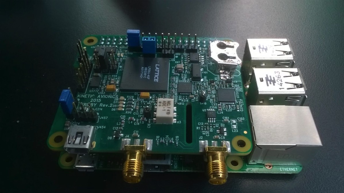
The TRILBY HAT is here !
A revolution in Raspberry Pi HAT functionality & pricing.
| Item | Connector | Description |
|---|---|---|
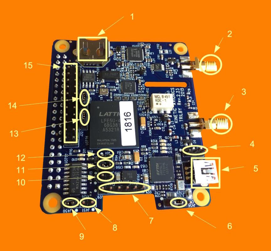
| 1 | B1 | Battery holder for real-time clock. Install CR1220 battery or equivalent with +ve terminal facing upwards, in order for the real-time clock to continue operating when the board is powered down. |
| 2 | J2 | SMA connector for VHF/UHF antenna |
| 3 | J4 | SMA connector for HF antenna |
| 4 | J457 | 3-pin audio PWM output header (pin 2 is GND, pin 1 and 3 are for the two audio channels) |
| 5 | J454 | USB mini connector Can be used to power the board and/or to program the FPGA from a personal computer |
| 6 | J456 | Power mode jumper Link pins 1 and 2 to power the Trilby board from Raspberry Pi Link pins 2 and 3 to power the Trilby board via its USB connector |
| 7 | J29 | 6-pin JTAG header which can be used to program the FPGA using a cable supplied by Lattice pin 1: +3.3V pin 2: TDI pin 3: TMS pin 4: TCK pin 5: TDO pin 6: GND |
| 8 | J451 | FPGA programming mode selection Do not install this jumper if FPGA is to be programmed using the USB port Install jumper when programming using a Lattice JTAG cable or from the Raspberry Pi |
| 9 | J450 | FPGA programming mode selection Install this jumper if programming the FPGA using the USB port or from the Raspberry Pi Remove jumper in order to program using a Lattice JTAG cable |
| 10 | J33 | FPGA PROGRAMING input. Short these two pins momentarily to trigger reloading of the FPGA firmware from the flash memory. |
| 11 | J30 | FPGA configuration mode, bit 0 (install jumper for normal operation) |
| 12 | J31 | FPGA configuration mode, bit 1 (do not install for normal operation) |
| 13 | J32 | FPGA configuration mode, bit 2 (install jumper for normal operation) |
| 14 | J26 | Install this jumper to enable the Raspberry Pi to write to the EEPROM |
| 15 | J458 | 24 pin GPIO Expansion header pin 1 and 2 are +5V supply pin 20, 23 and 24 are GND pin 22 is an active-low reset signal (short to GND to reset the FPGA) when using demo firmware all other pins are connected directly to IO pins on the FPGA |
T
Mission

150kHz to 1000MHz+
Software Defined Radio
Software Defined Radio

HF Up Converter

Real Time Clock

Dual Audio Output Channels / Stereo Capable

4 Coloured LEDs

GPIO FPGA Breakout Connector

Lattice ECP5-45 FPGA

Use Standalone or with Raspberry Pi
Our mission is to be the pre-eminent designer and developer of Avionic, Marine and Software Defined Radio solutions for surveillance monitoring, recording and analysis.
